分享
举报
评价

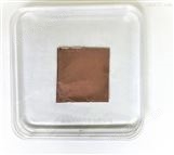
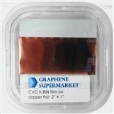
基于铜基的单层氮化硼薄膜(5*2.5cm)
| 参考价 | 面议 |
具体成交价以合同协议为准
- 公司名称 上海巨纳科技有限公司
- 品牌
- 型号
- 所在地
- 厂商性质 经销商
- 更新时间 2020/12/26 13:52:17
- 访问次数 310
联系方式:袁经理 13761090949 查看联系方式
联系我们时请说明是仪器网上看到的信息,谢谢!
| 参考价 | 面议 |
联系方式:袁经理 13761090949 查看联系方式
联系我们时请说明是仪器网上看到的信息,谢谢!
Single layer h-BN (Boron Nitride) film grown in copper foil.h-BN is an insulator with a direct band gap of 5.97 eV. Due to its strong covalent sp2 bonds in the plane, the in-plane mechanical strength
Single layer h-BN (Boron Nitride) film grown in copper foil.
h-BN is an insulator with a direct band gap of 5.97 eV. Due to its strong covalent sp2 bonds in the plane, the in-plane mechanical strength and thermal conductivity of h-BN has been reported to be close to that of graphene. h-BN has an even higher chemical stability than graphene; it can be stable in air up to 1000 °C (in contrast, for graphene the corresponding temperature is 600 °C).
During Chemical Vapor Deposition, BN is grown on both sides of the copper foil
Specifications:
Close to complete coverage (90-95%), with some minor holes
Thickness of the copper foil is 20 microns
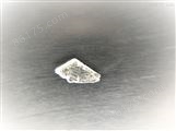
High crystalline quality, see SAD (Selected area [electron] diffraction) data
Quality is confirmed by TEM. TEM shows perfect hexagonal structure.
TEM image of perfect hexagonal structure
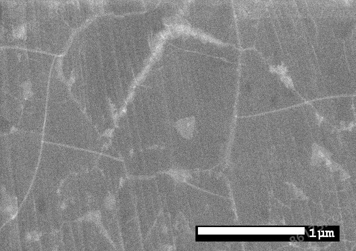
On SEM image (below), BN is seen as wrinkles on top of the copper foil.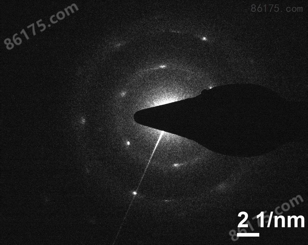
SAD data of h-BN
If transferred onto an SiO2 substrate, the BN film may be seen as a white film. However, it is difficult to recognize the BN film on copper using a microscope.
Absorbance data BN on copper
|
|
|
|
|
|
*您想获取产品的资料:
个人信息: