分享
举报
评价
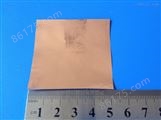
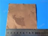
基于蓝宝石衬底的全区域覆盖的单层二硫化铼
| 参考价 | 面议 |
具体成交价以合同协议为准
- 公司名称 上海巨纳科技有限公司
- 品牌
- 型号
- 所在地
- 厂商性质 经销商
- 更新时间 2020/12/27 1:21:57
- 访问次数 441
联系方式:袁经理 13761090949 查看联系方式
联系我们时请说明是仪器网上看到的信息,谢谢!
| 参考价 | 面议 |
联系方式:袁经理 13761090949 查看联系方式
联系我们时请说明是仪器网上看到的信息,谢谢!
This product contains full area coverage ReS2 monolayers on c-cut sapphire substrates.
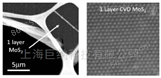
This product contains full area coverage ReS2 monolayers on c-cut sapphire substrates. Sample size measures 1cm in size and the entire sample surface contains monolayer thick ReS2 sheet. Synthesized full area coverage monolayer ReS2 is highly crystalline, some regions also display significant crystalline anisotropy.
Sample Properties.
Sample size | 1cm x 1cm square shaped |
Substrate type | Sapphire c-cut (0001) |
Coverage | Full monolayer coverage |
Electrical properties | 1.6 eV Anisotropic Semiconductor (Indirect Bandgap) |
Crystal structure | Distorted Tetragonal Phase (1T’) |
Unit cell parameters | a = 0.630, b = 0.638 nm, c = 0.643 nm α = 106.74°, β = 119.03°, γ = 89.97° |
Production method | Atmospheric Pressure Chemical Vapor Deposition (APCVD) |
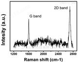
Characterization methods | Raman, angle resolved Raman spectroscopy, photoluminescence, absorption spectroscopy TEM, EDS |
Specifications
1) Full coverage * monolayer ReS2 uniformly covered across c-cut sapphire.
2) . One centimeter in size. Larger sizes up to 2-inch wafer-scale available upon requests.
3) Atomically smooth surface with roughness < 0.2 nm.
4) Highly uniform surface morphology. ReS2 monolayers uniformly cover across the sample.
5) 99.9995% purity as determined by nano-SIMS measurements
6) Repeatable Raman and photoluminescence response
7) High crystalline quality, Raman response, and photoluminescence emission comparable to single crystalline monolayer flakes.
8) c-cut Sapphire but our research and development team can transfer ReS2 monolayers onto variety of substrates including PET, quartz, and SiO2/Si without significant compromisation of material quality.
9) ReS2 monolayers do not contain intentional dopants or defects. However, our technical staff can produce defected ReS2 using α-bombardment technique.
Supporting datasets [for * Full area ReS2 monolayers on c-cut Sapphire]
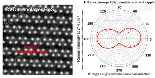
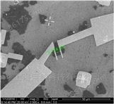
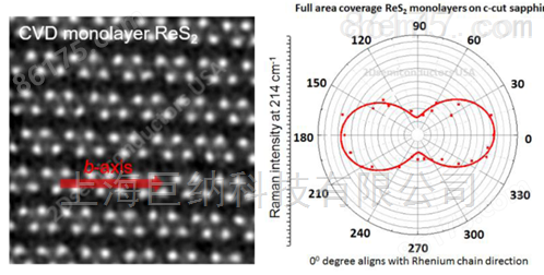
Transmission electron images (TEM) and angle resolved Raman spectroscopy measurements acquired from CVD grown full area coverage ReS2 monolayers on c-cut sapphire confirming crystalline anisotropy.
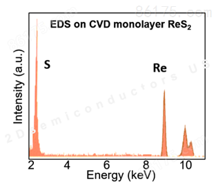
Energy dispersive X-ray spectroscopy (EDX) characterization on CVD grown full area coverage monolayer ReS2 on c-cut sapphire
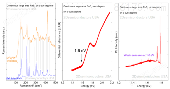
Raman spectroscopy measurement confirm monolayer nature of the CVD grown samples. Differential reflectance measurements clearly show band gap at 1.6 eV for ReS2 consistent with the existing literature values. PL spectrum only display weak emission at 1.6 eV but significantly stronger at lower temperatures.

|
|
|
|
|
|
*您想获取产品的资料:
个人信息: